

Products

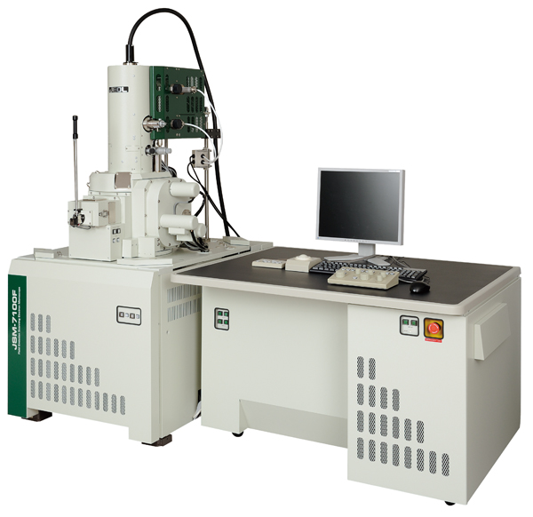
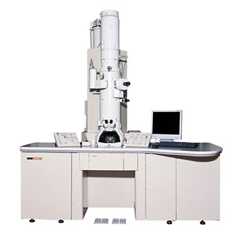
JSM-7100FA Entry-Level FE SEM
Full-featured Analytical Field Emission SEM for Budget-Conscious Labs
Step up to a full-featured Field Emission SEM for high resolution imaging and analysis. By combining large beam currents with a small probe size at ANY accelerating voltage, it dramatically increases analytical resolution to the sub 100nm scale. The JSM-7100FA incorporates the JEOL EDS and backscattered electron detector (BSED) in an easily affordable FE SEM that is ideal for the lab moving up to utilize the power of Field Emission SEM for the first time.
With the JEOL Energy Dispersive X-Ray Analysis (EDS) system, the JSM-7100FA seamlessly shifts from high spatial resolution imaging to high-precision quantitative and qualitative analysis modes. The dry Silicon Drift Detector with built-in retraction features an active area of 10mm2, energy resolution ≤129eV (FWHM at Mn Kα), and an ultra-thin film window for detection of elements ranging from Be to U.
Key Features
- High resolution imaging and nanoanalysis for structures, surface details, and magnetic samples
- Solid-state backscatter detector (standard)
- Outstanding high and low kV performance
- High stable current with double condenser lens and aperture angle control lens
- 10mm2 Dry Silicon Drift Detector EDS
- BF STEM converter holder for STEM-in-SEM imaging of electron transparent samples utilizing the LED detector
- Multi-port chamber for in situ nanolab utility
Specification:
| SEI Resolution | 1.2nm at 30kV
1.5nm at 15kV 3.0nm at 1.0kV 3.0nm (15kV, 5nA, 10mm WD) |
| Accelerating Voltage | 0.5 to 2.9kV (in 10V steps)
(0.2 to 2.9kV in GBL mode) 2.9 to 30kV (in 100V steps) |
| Magnification Range
| 10X - 1,000,000X |
| Probe Current Range
| 1pA to > 200n |


Support online


Hãy liên hệ với chúng tôi để nhận được tư vấn - hỗ trợ tốt nhất về các sản phẩm và dịch vụ của TLT.
Hot line: 04.36642336